- 您现在的位置:买卖IC网 > Sheet目录1991 > CS5381-KSZ (Cirrus Logic Inc)IC ADC AUD 120DB 192KHZ 24-SOIC
IDT / ICS 3.3V, 2.5V LVPECL CLOCK GENERATOR
8
ICS843031AG-01 REV. A NOVEMBER 11, 2008
ICS843031-01
FEMTOCLOCKS CRYSTAL-TO-3.3V, 2.5V LVPECL CLOCK GENERATOR
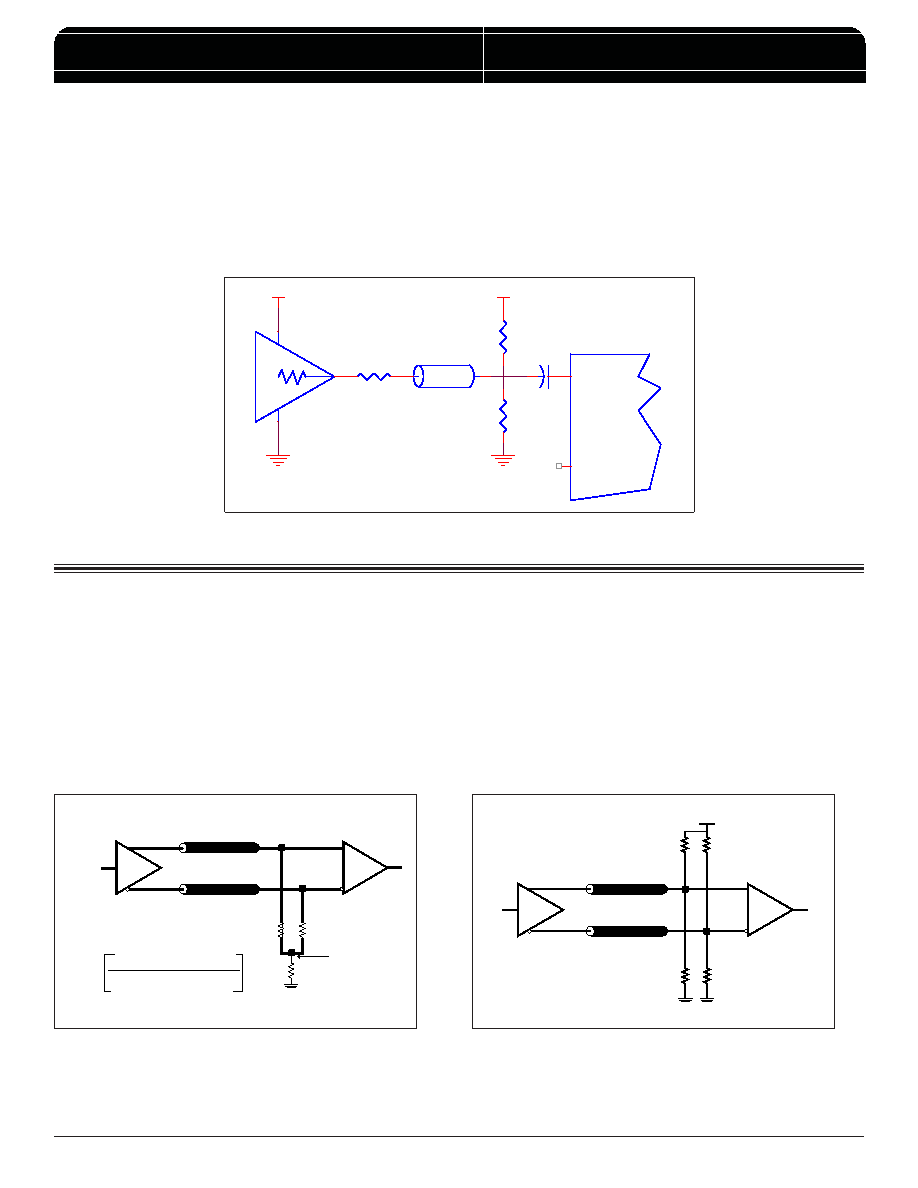
LVCMOS TO XTAL INTERFACE
The XTAL_IN input can accept a single-ended LVCMOS signal
through an AC coupling capacitor. A general interface diagram is
shown in
Figure 3. The XTAL_OUT pin can be left floating. The
input edge rate can be as slow as 10ns. For LVCMOS inputs, it is
recommended that the amplitude be reduced from full swing to
half swing in order to prevent signal interference with the power
rail and to reduce noise. This configuration requires that the output
FIGURE 3. GENERAL DIAGRAM FOR LVCMOS DRIVER TO XTAL INPUT INTERFACE
impedance of the driver (Ro) plus the series resistance (Rs) equals
the transmission line impedance. In addition, matched termination
at the crystal input will attenuate the signal in half. This can be
done in one of two ways. First, R1 and R2 in parallel should equal
the transmission line impedance. For most 50
Ω applications, R1
and R2 can be 100
Ω. This can also be accomplished by removing
R1 and making R2 50
Ω.
R2
Zo = 50
VDD
Ro
Zo = Ro + Rs
R1
VDD
XTAL_IN
XTAL_OUT
.1uf
Rs
TERMINATION FOR 3.3V LVPECL OUTPUTS
The clock layout topology shown below is a typical termination
for LVPECL outputs. The two different layouts mentioned are
recommended only as guidelines.
FOUT and nFOUT are low impedance follower outputs that gen-
erate ECL/LVPECL compatible outputs. Therefore, terminating
resistors (DC current path to ground) or current sources must be
used for functionality. These outputs are designed to drive 50
Ω
FIGURE 4B. LVPECL OUTPUT TERMINATION
FIGURE 4A. LVPECL OUTPUT TERMINATION
transmission lines. Matched impedance techniques should be
used to maximize operating frequency and minimize signal dis-
tortion.
Figures 4A and 4B show two different layouts which are
recommended only as guidelines. Other suitable clock layouts
may exist and it would be recommended that the board design-
ers simulate to guarantee compatibility across all printed circuit
and clock component process variations.
V
CC - 2V
50
Ω
50
Ω
RTT
Z
o = 50Ω
Z
o = 50Ω
FOUT
FIN
RTT =
Z
o
1
((V
OH + VOL) / (VCC – 2)) – 2
3.3V
125
Ω
125
Ω
84
Ω
84
Ω
Z
o = 50Ω
Z
o = 50Ω
FOUT
FIN
发布紧急采购,3分钟左右您将得到回复。
相关PDF资料
CS53L21-CNZR
IC ADC STEREO 24BIT 98DB 32-QFN
CS5509-ASZR
IC ADC 16BIT SGL SUPP 16-SOIC
CS5512-BSZ
IC ADC 20BIT EXTERNAL OSC 8-SOIC
CS5526-BSZR
IC ADC 20BIT W/4BIT LATCH 20SSOP
CS5528-ASZR
IC ADC 24BIT 8CH 24-SSOP
CS5529-ASZR
IC ADC 16BIT W/6BIT LATCH 20SSOP
CS5530-ISZR
IC ADC 24BIT 1CH W/LNA 20-SSOP
CS5534-ASZR
IC ADC 24BIT 4CH W/LNA 24-SSOP
相关代理商/技术参数
CS5381-KSZR
功能描述:音频模/数转换器 IC IC 120dB 192kHz Multi-Bit ADC RoHS:否 制造商:Wolfson Microelectronics 转换速率: 分辨率: ADC 输入端数量: 工作电源电压: 最大工作温度: 最小工作温度: 安装风格: 封装 / 箱体: 封装:
CS5381-KZR
制造商:Cirrus Logic 功能描述:T&R VERSION OF CS5381-KZ - Tape and Reel
CS5381-KZZ
功能描述:音频模/数转换器 IC 120dB 192kHz Multi-Bit ADC RoHS:否 制造商:Wolfson Microelectronics 转换速率: 分辨率: ADC 输入端数量: 工作电源电压: 最大工作温度: 最小工作温度: 安装风格: 封装 / 箱体: 封装:
CS5381-KZZR
功能描述:音频模/数转换器 IC IC 120dB 192kHz Multi-Bit ADC RoHS:否 制造商:Wolfson Microelectronics 转换速率: 分辨率: ADC 输入端数量: 工作电源电压: 最大工作温度: 最小工作温度: 安装风格: 封装 / 箱体: 封装:
CS5385-000
制造商:TE Connectivity 功能描述:MT1000-1/4-0-16.75IN - Bulk
CS5388-000
制造商:TE Connectivity 功能描述:Cable Accessories Transition 制造商:TE Connectivity 功能描述:302A821-4-0
CS5389-KP
制造商:未知厂家 制造商全称:未知厂家 功能描述:Analog-to-Digital Converter, 18-Bit
CS5390-KP
制造商:未知厂家 制造商全称:未知厂家 功能描述:Analog-to-Digital Converter, 20-Bit